- 您现在的位置:买卖IC网 > Sheet目录866 > LMZ14203EXTTZE/NOPB (National Semiconductor)IC BUCK SYNC ADJ 3A TO-PMOD-7
�� �
�
�LMZ14203EXT�
�www.ti.com�
�I� LR� P-P� =� V� O� *(V� IN� -� V� O� )/(6.8μH*f� SW� *V� IN� )�
�where�
�SNVS666F� –� JUNE� 2010� –� REVISED� OCTOBER� 2013�
�?�
�V� IN� is� the� maximum� input� voltage�
�?�
�f� SW� is� determined� from� Equation� 7�
�(14)�
�If� the� output� current� I� O� is� determined� by� assuming� that� I� O� =� I� L� ,� the� higher� and� lower� peak� of� I� LR� can� be�
�determined.� Be� aware� that� the� lower� peak� of� I� LR� must� be� positive� if� CCM� operation� is� required.�
�POWER� DISSIPATION� AND� BOARD� THERMAL� REQUIREMENTS�
�For� the� design� case� of� V� IN� =� 24V,� V� O� =� 3.3V,� I� O� =� 3A,� T� AMB(MAX)� =� 85°C� ,� and� T� JUNCTION� =� 125°C,� the� device� must�
�see� a� thermal� resistance� from� case� to� ambient� of:�
�θ� CA� <� (T� J-MAX� —� T� AMB(MAX)� )� /� P� IC-LOSS� -� θ� JC�
�(15)�
�Given� the� typical� thermal� resistance� from� junction� to� case� to� be� 1.9� °C/W.� Use� the� 85°C� power� dissipation� curves�
�in� the� Typical� Performance� Characteristics� section� to� estimate� the� P� IC-LOSS� for� the� application� being� designed.� In�
�this� application� it� is� 2.25W.�
�θ� CA� <� (125� —� 85)� /� 2.25W� —� 1.9� =� 15.8�
�To� reach� θ� CA� =� 15.8,� the� PCB� is� required� to� dissipate� heat� effectively.� With� no� airflow� and� no� external� heat,� a�
�good� estimate� of� the� required� board� area� covered� by� 1� oz.� copper� on� both� the� top� and� bottom� metal� layers� is:�
�Board� Area_cm� 2� >� 500°C� x� cm� 2� /W� /� θ� CA�
�(16)�
�As� a� result,� approximately� 31.5� square� cm� of� 1� oz� copper� on� top� and� bottom� layers� is� required� for� the� PCB�
�design.� The� PCB� copper� heat� sink� must� be� connected� to� the� exposed� pad.� Approximately� thirty� six,� 8mils� thermal�
�vias� spaced� 59mils� (1.5� mm)� apart� must� connect� the� top� copper� to� the� bottom� copper.� For� an� example� of� a� high�
�thermal� performance� PCB� layout,� refer� to� the� Evaluation� Board� application� note� AN-2024� SNVA422� .�
�PC� BOARD� LAYOUT� GUIDELINES�
�PC� board� layout� is� an� important� part� of� DC-DC� converter� design.� Poor� board� layout� can� disrupt� the� performance�
�of� a� DC-DC� converter� and� surrounding� circuitry� by� contributing� to� EMI,� ground� bounce� and� resistive� voltage� drop�
�in� the� traces.� These� can� send� erroneous� signals� to� the� DC-DC� converter� resulting� in� poor� regulation� or� instability.�
�Good� layout� can� be� implemented� by� following� a� few� simple� design� rules.�
�V� IN�
�VIN�
�LMZ14203EXT�
�VOUT�
�V� O�
�High�
�C� in1�
�Loop� 1�
�di/dt�
�GND�
�Loop� 2�
�C� O1�
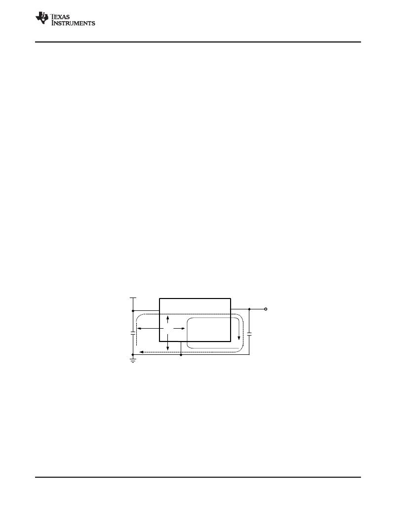
�1.� Minimize� area� of� switched� current� loops.�
�From� an� EMI� reduction� standpoint,� it� is� imperative� to� minimize� the� high� di/dt� paths� during� PC� board� layout.� The�
�high� current� loops� that� do� not� overlap� have� high� di/dt� content� that� will� cause� observable� high� frequency� noise� on�
�the� output� pin� if� the� input� capacitor� (Cin1)� is� placed� at� a� distance� away� from� the� LMZ14203EXT.� Therefore� place�
�C� IN1� as� close� as� possible� to� the� LMZ14203EXT� VIN� and� GND� exposed� pad.� This� will� minimize� the� high� di/dt� area�
�and� reduce� radiated� EMI.� Additionally,� grounding� for� both� the� input� and� output� capacitor� should� consist� of� a�
�localized� top� side� plane� that� connects� to� the� GND� exposed� pad� (EP).�
�2.� Have� a� single� point� ground.�
�The� ground� connections� for� the� feedback,� soft-start,� and� enable� components� should� be� routed� to� the� GND� pin� of�
�the� device.� This� prevents� any� switched� or� load� currents� from� flowing� in� the� analog� ground� traces.� If� not� properly�
�handled,� poor� grounding� can� result� in� degraded� load� regulation� or� erratic� output� voltage� ripple� behavior.� Provide�
�the� single� point� ground� connection� from� pin� 4� to� EP.�
�Copyright� ?� 2010–2013,� Texas� Instruments� Incorporated�
�Product� Folder� Links:� LMZ14203EXT�
�Submit� Documentation� Feedback�
�15�
�发布紧急采购,3分钟左右您将得到回复。
相关PDF资料
LNC2W153MSEJ
CAP ALUM 15000UF 450V 20% SCREW
LNK2H822MSEJ
CAP ALUM 8200UF 500V 20% SCREW
LNT2H103MSEJ
CAP ALUM 10000UF 500V 20% SCREW
LNX2J562MSEK
CAP ALUM 5600UF 630V 20% SCREW
LNY2W153MSEJ
CAP ALUM 15000UF 450V 20% SCREW
LP122M250H9P3
CAP ALUM 1200UF 250V 20% SNAP
LPW332M2AP45V-W
CAP ALUM 3300UF 100V 20% SNAP
LPX222M200H9P3
CAP ALUM 2200UF 200V 20% SNAP
相关代理商/技术参数
LMZ14203EXTTZNOPB
制造商:National Semiconductor 功能描述:Simple Switcher Power Module 7-Pin TO-PMOD T/R
LMZ14203EXTTZX/NOPB
功能描述:直流/直流开关转换器
RoHS:否 制造商:STMicroelectronics 最大输入电压:4.5 V 开关频率:1.5 MHz 输出电压:4.6 V 输出电流:250 mA 输出端数量:2 最大工作温度:+ 85 C 安装风格:SMD/SMT
LMZ14203H
制造商:NSC 制造商全称:National Semiconductor 功能描述:Evaluation Board modules for high output voltage are easy-to-use DC-DC
LMZ14203H_1106
制造商:NSC 制造商全称:National Semiconductor 功能描述:3A SIMPLE SWITCHER? Power Module for High Output Voltage
LMZ14203HEVAL/NOPB
功能描述:电源管理IC开发工具 LMZ14203H EVAL BOARD
RoHS:否 制造商:Maxim Integrated 产品:Evaluation Kits 类型:Battery Management 工具用于评估:MAX17710GB 输入电压: 输出电压:1.8 V
LMZ14203HTZ
制造商:Texas Instruments 功能描述:POWER MODULE, 42V, 3A, 7TOPMOD 制造商:Texas Instruments 功能描述:POWER MODULE, 42V, 3A, 7TOPMOD; Primary Input Voltage:42V; No. of Outputs:1; Output Voltage:30V; Output Current:3A; Voltage Regulator Case Style:TO-PMOD; No. of Pins:7; Operating Temperature Min:-40C; Operating Temperature ;RoHS Compliant: Yes
LMZ14203HTZ/NOPB
功能描述:直流/直流开关转换器 42V,3A PWR MODULE
RoHS:否 制造商:STMicroelectronics 最大输入电压:4.5 V 开关频率:1.5 MHz 输出电压:4.6 V 输出电流:250 mA 输出端数量:2 最大工作温度:+ 85 C 安装风格:SMD/SMT
LMZ14203HTZE
制造商:NSC 制造商全称:National Semiconductor 功能描述:3A SIMPLE SWITCHER Power Module for High Output